Chemical Vapor Deposition CVD Furnace
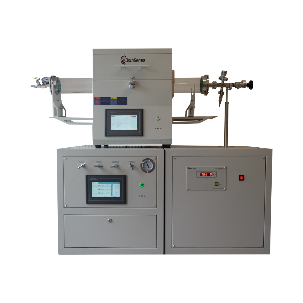
CVD (CHEMICAL VAPOR DEPOSITION) systems are one of the coating systems used in thin film studies, Li-ion battery studies, graphene-based studies and R&D studies. Optosense brand CVD systems are a complete system consisting of a tube furnace, 2-4 channel MFC unit and vacuum pump. Since each component of the system is designed to be added to each other later, your heat treatment processes that start with a tube furnace can be transformed into a CVD system with the MFC unit that can be added later. Each unit of our CVD systems can be produced according to the specifications requested by the user.
SALE PRICE: RFQ
TOUCH SCREEN CONTROL
MAXIMUM TEMPATURE: 1200 °C – 1400 °C – 1700 °C
WORK TEMPATURE: 1100 °C – 1300 °C – 1600 °C
HEAT ZONE LENGHT: 200 – 300 – 400 – 500 MM
TUBE MATERIAL: HIGH PURITY QUARTZ OR ALUMINA
MATERIALS RESEARCH AND TESTING
CHEMICAL SYNTHESIS
CERAMIC AND GLASS PROCESSING
CRYSTAL GROWTH
SEMICONDUCTOR FABRICATION
HEAT TREAMENT
BRAZING AND SOLDERING
CARBON FIBER PRODUCTION
ENVIRONMENTAL TESTING
DRYING AND DEHYDRATION
AEROSPACE AND DEFENSE
RESEARCH AND DEVELOPMENT
EDUCATION
FLANGES
VACUUM GAUGE
VACUUM PUMP
TURBO VACUUM PUMP
MECHANICAL PUMP
A Chemical Vapor Deposition (CVD) furnace is a type of equipment used in materials science and semiconductor manufacturing to deposit thin films or coatings onto substrates through a chemical reaction in the vapor phase. CVD is a widely used technique for producing high-quality thin films with precise control over thickness, composition, and other properties.
Working Principle Of Chemical Vapor Deposition CVD Furnaces
The working principle of a Chemical Vapor Deposition (CVD) furnace involves the deposition of a thin film or coating onto a substrate through the chemical reaction of precursor gases in the vapor phase. Here’s a step-by-step explanation of the working principle of a typical CVD furnace:
–Substrate Preparation: The substrate onto which the thin film or coating will be deposited is prepared. It is cleaned and often treated to ensure proper adhesion and compatibility with the desired material to be deposited.
–Precursor Gas Introduction: One or more precursor gases containing the elements or compounds needed for the thin film deposition are introduced into the CVD furnace chamber. These precursor gases are typically in a volatile form and can include organometallic compounds, halides, or other chemicals. The choice of precursor gases depends on the material composition desired in the thin film.
–Heating the Furnace: The furnace chamber is heated to a specific temperature, which is critical to the CVD process. The temperature is carefully controlled and maintained because it determines the rate of chemical reactions and the properties of the resulting thin film.
–Chemical Reactions: As the precursor gases are heated, they break down and undergo chemical reactions in the vapor phase. These reactions may involve the dissociation of molecules, the formation of intermediates, and the transport of atoms or molecules to the substrate surface.
–Transport of Species: The products of the chemical reactions, which are often volatile compounds or radicals, are transported toward the substrate surface by diffusion and convection. The species reach the substrate in a highly reactive state.
–Surface Reaction and Film Deposition: When the reactive species come into contact with the cooler substrate surface, they react with the surface atoms or molecules, leading to the deposition of a solid thin film or coating. The deposition process can involve the adsorption of atoms or molecules onto the substrate and the formation of chemical bonds.
–Growth and Control: The deposition process continues, and the thin film thickness increases over time. The process is carefully controlled to achieve the desired film thickness, composition, and properties. Parameters such as temperature, gas flow rates, and reaction times are adjusted as needed.
–Byproduct Removal: Byproducts of the chemical reactions and any unreacted precursor gases are removed from the furnace chamber through an exhaust system. This ensures that the deposition process remains clean and that unwanted contaminants do not affect the thin film’s quality.
–Cooling and Substrate Retrieval: Once the desired thin film thickness is achieved, the furnace may be cooled down, and the substrate is retrieved. The thin film is now deposited on the substrate and can be further processed or used in various applications.
The working principle of a CVD furnace is highly dependent on precise temperature control, gas chemistry, and deposition conditions to produce thin films with specific properties, making it a versatile and widely used technique in industries such as semiconductor manufacturing, optics, and materials science.
What are the usage areas of Chemical Vapor Deposition CVD furnaces?
Chemical Vapor Deposition (CVD) furnaces are versatile tools used in various industries and research fields due to their ability to deposit thin films and coatings with precise control over composition and properties. Here are some of the usage areas of CVD furnaces:
–Semiconductor Manufacturing: CVD is widely employed in the semiconductor industry to deposit thin films of materials like silicon dioxide (SiO2), silicon nitride (Si3N4), and various metals onto silicon wafers. These thin films are essential for the fabrication of integrated circuits and microelectronics.
–Optical Coatings: CVD is used to produce anti-reflective coatings, optical filters, and mirrors for optical devices such as lenses, camera lenses, eyeglasses, and telescope lenses. These coatings improve light transmission, reduce glare, and enhance optical performance.
–Photovoltaics: In the production of solar cells, CVD is used to deposit thin films of semiconductor materials like amorphous silicon (a-Si), cadmium telluride (CdTe), and copper indium gallium selenide (CIGS) to convert sunlight into electricity.
–Thin-Film Transistors (TFTs): CVD is utilized to create thin-film transistor layers, which are crucial components in flat-panel displays (e.g., LCD and OLED screens), organic electronics, and flexible displays.
–MEMS and NEMS Devices: Micro-electromechanical systems (MEMS) and nanoelectromechanical systems (NEMS) devices are fabricated using CVD to deposit materials like silicon carbide (SiC), silicon nitride (Si3N4), and metals for sensors, actuators, and microstructures.
–Advanced Materials: CVD is used to produce advanced materials like graphene, carbon nanotubes, and diamond films with unique electrical, mechanical, and thermal properties for applications in electronics, sensors, and cutting tools.
–Corrosion and Wear Protection: CVD coatings are applied to protect materials from corrosion, wear, and erosion. For example, titanium nitride (TiN) and diamond-like carbon (DLC) coatings can be deposited using CVD for this purpose.
–Aerospace and Defense: CVD is used to manufacture components and coatings for aerospace and defense applications, including thermal barriers, protective coatings, and high-temperature materials for jet engines and missile systems.
–Biomedical Devices: CVD is employed to deposit biocompatible coatings on medical implants and devices, improving their compatibility with the human body and reducing the risk of rejection or infection.
–Laboratory Research: CVD furnaces are used in research and development laboratories for exploring new materials, studying their properties, and developing novel applications in areas such as materials science, chemistry, and physics.
–Surface Modification: CVD can be used to modify the surface properties of materials, such as adding hydrophobic or hydrophilic coatings, to enhance their performance in various applications.
–Fuel Cells: CVD is used to deposit electrode materials and electrolytes in solid oxide fuel cells (SOFCs) and other types of fuel cells, enabling efficient energy conversion.
The versatility of CVD technology makes it valuable across a wide range of industries, from electronics and optics to energy, aerospace, and healthcare. Researchers and engineers continue to develop new applications and materials using CVD processes, expanding its utility even further.