Sputter Coating
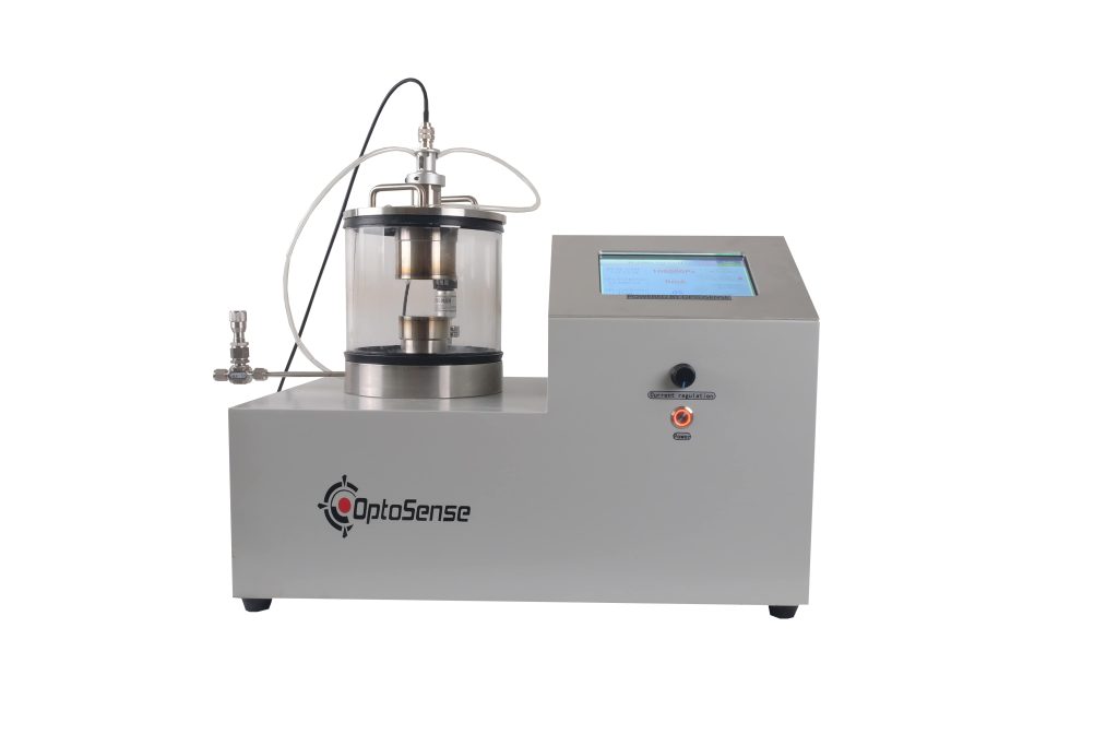
This equipment is a desktop single sputter head magnetron sputtering coating machine. The miniaturized design of the equipment limits the appearance of the equipment to the desktop level, greatly reducing the installation site requirements. The Desktop single sputter head magnetron sputtering coater equipment is equipped with a DC power supply, which can be used for sputtering metal materials and has the characteristics of fast speed and low temperature rise.
SALE PRICE: RFQ
Sputter coating, also known as physical vapor deposition (PVD) sputtering, is a process used in materials science and surface engineering to deposit a thin film of one material onto the surface of another material. This technique is commonly employed in various applications, including electronics, optics, semiconductor manufacturing, and research.
Working Principle Of Sputter Coating
The working principle of sputter coating, also known as physical vapor deposition (PVD) sputtering, involves the generation of a plasma and the ejection of material from a target onto a substrate in a vacuum chamber. Here’s a step-by-step explanation of the working principle:
–Preparation: The object to be coated, called the substrate, is placed inside a vacuum chamber. The substrate is often cleaned and prepared to ensure proper adhesion of the deposited material.
–Target Material: The material you want to deposit as a thin film, known as the target, is also placed inside the vacuum chamber. The target is typically made of the same material you want to deposit.
–Gas Filling: The vacuum chamber is evacuated to create a low-pressure environment, typically in the range of 10^-2 to 10^-3 torr. This low-pressure environment is necessary to reduce gas collisions and to minimize contamination during the sputtering process. A noble gas, such as argon, is introduced into the chamber as a process gas.
–Plasma Generation: A strong electric field is applied to the target material. This electric field ionizes the process gas, typically argon, and creates a plasma within the vacuum chamber. The plasma is a highly energized and ionized gas consisting of positively charged ions and electrons.
–Sputtering: The positively charged ions in the plasma are attracted to the negatively charged target material. These ions gain energy and momentum as they travel towards the target. When the ions collide with the target surface, they transfer their energy and momentum to the target atoms. This process causes target atoms to be ejected from the target surface. The ejected atoms form a flux of particles that travel in straight-line trajectories.
–Thin Film Deposition: The ejected target atoms travel in straight lines and deposit on the substrate material. As these atoms accumulate on the substrate, they form a thin film with properties similar to the target material. The thickness and composition of the thin film can be controlled by adjusting the deposition time, the power applied to the target, and other process parameters.
The key to sputter coating is the controlled generation of a plasma and the precise manipulation of process parameters to achieve the desired film properties. Sputter coating allows for the deposition of thin films of various materials, including metals, semiconductors, and dielectrics, making it a versatile and widely used technique in materials science, electronics, and various industrial applications. This process is valuable in industries such as semiconductor manufacturing, optics, electronics, and surface engineering, where precise control over thin film properties is crucial.
What are the usage areas of the sputter coating?
Sputter coating, also known as physical vapor deposition (PVD) sputtering, has a wide range of usage areas across various industries due to its ability to deposit thin films with precise control over thickness and composition. Some of the common usage areas of sputter coating include:
–Semiconductor Manufacturing: Sputter coating is extensively used in the semiconductor industry to create thin films for integrated circuits, sensors, and other semiconductor devices. It can be used to deposit metal and dielectric films on semiconductor wafers, aiding in the production of electronic components.
–Optics and Thin-Film Coatings: Sputter coating is used to manufacture anti-reflective coatings, reflective coatings, and beam splitters for optical components such as lenses, mirrors, and filters. It helps improve light transmission, reduce glare, and enhance optical performance.
–Solar Cells: Sputter coating is utilized in the production of thin-film solar cells, including amorphous silicon, cadmium telluride, and copper indium gallium selenide (CIGS) solar cells. These thin films help capture and convert sunlight into electrical energy.
–Magnetic Storage Media: Sputter coating is used to deposit magnetic thin films on hard disk drives, allowing for high-density data storage. These thin films are crucial for the read/write heads of hard drives.
–Microelectronics and MEMS: Microelectromechanical systems (MEMS) often require precise thin film depositions, and sputter coating is used in their fabrication. It is employed in the creation of MEMS devices like accelerometers, microsensors, and microactuators.
–Packaging and Display Technologies: Sputter coating is used to create conductive and transparent films on glass and plastic substrates for applications in packaging, touch screens, flat-panel displays (e.g., LCDs and OLEDs), and electrochromic windows.
–Cutting Tools and Tribology: Sputter-coated thin films can enhance the wear resistance and lubrication properties of cutting tools and other mechanical components, improving their durability and performance.
–Biomedical Devices: Sputter coating can be used to deposit bioactive coatings on medical implants, improving their biocompatibility and promoting tissue integration. It is also used to create conductive and electrode materials for medical devices.
–Protective and Decorative Coatings: Sputter coating is employed to deposit protective and decorative coatings on a wide range of objects, from consumer goods (e.g., jewelry, eyeglass frames) to automotive parts (e.g., decorative trims, reflectors).
–Research and Development: Sputter coating is a valuable tool in research laboratories for a wide range of scientific experiments, including material characterization, sample preparation, and the fabrication of specialized materials.
–Thin-Film Deposition for Research: Sputter coating is used for thin-film deposition in a wide range of scientific research applications, including material science, surface science, and thin-film physics.
The versatility of sputter coating, along with its ability to create thin films with precise control over their properties, makes it a vital process in various industries and research fields. It plays a critical role in improving the functionality, durability, and performance of materials and devices in these areas.